Our Applications

Via Drilling

NSI LASER is continually developing and adding new hole drilling processes and capabilities. Typically we can drill material that range in thickness from very thin films to several mm’s on a high speed setup that can drill thousands holes quickly and repeatably. Depending on the material and specifications, we will choose the optimized tool to drill the holes.

Drilling Control

75um Via

Blind Via

Blind via top focus 
Blind via bottom focus (with UV laser cleaning process)
 

Via Drill with hybrid UV CO2 laser machine

20um via hole, 45um depth, 2:1 aspect ratio made using shots

Microvias hole diameters are limited by aspect ratio (hole depth to hole diameter). 

Through Hole Drilling

Through hole diameter 150um
Through hole diameter 250um
 
Through hole diameter 500um
Through hole diameter 1200um
 

Isolation Routing

With NSIconverterTM, we can convert Gerber files into isolation routing files. By optimizing the routing path to become compatible with the laser route, we can achieve higher accuracy and quality. Our machine can process fine line/space as small as 15 micron.

Isolation Routing for FPC/COF production

10um trace and 15um space
Completed CoF panel

Optimal tool by shop

HDI pads and space
Feet isolation
 

Cutting & Depaneling

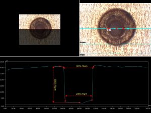
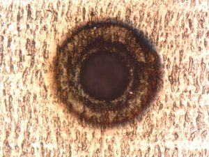
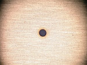
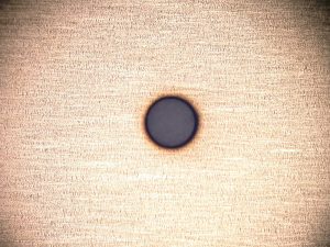
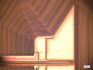
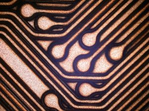
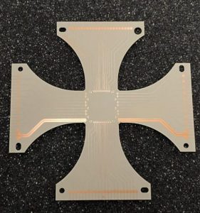
Thick PCB depaneling
Our system can implement the depaneling process on various PCB material using UV lasers that meet the demand of high-volume PCB manufacturing. Our system can process PCB with minimal carbonization.
 
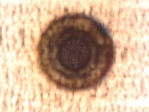
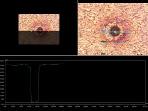
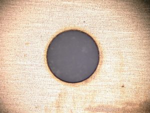
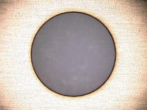
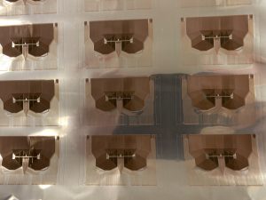
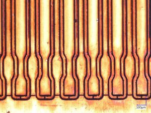
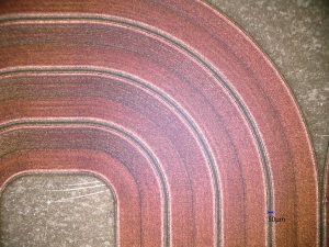
FPC and thin film cutting
Singulation-flex and rigid-flex circuits often requires cutting patterns that allows for more circuits on a single panel, which increases the net usable area. With Our NSIcoverter software, our system can do precise free form cutting by customers’ Gerber files.

Depaneling

Flex depaneling

Skiving / Hatching

Our machines can remove material to reveal fiducial marks through both hatching and skiving. Our hatch function can process complex patterns to create prototype PCB and allow you to control the overlap to help develop finer recipes. 

Skiving and Hatching

Skiving, used for exposing fiducials for panel registration
Curved hatching product

Wafer Scribing

Our machines also have scribing functionality that enables you to mark or label your materials.

Scribing on solar wafer

Scribing line and pattern on solar wafer

High circularity, no overlap when scribing in straight line for PERC application.

Do you still have more questions?

error: Content is protected !!