Transitioning From Mechanical to Laser Micro Machining

Laser processing systems are costly due to the expensive components and the laser itself. Don’t be scared by the price tag though, there are ways to go around it such as special financing or purchasing older generation or refurbished systems. If there aren’t any available used or refurbished options, opt towards dual laser for more versatility. One system with a combination of lasers enable multiple processes in one set-up and will save costs compared to buying two lasers and will enhance your material processing capability if you use two different wavelengths and laser types.

Return On Investment
It might be a good investment to buy an inhouse laser system if there’s such a high demand that almost all the jobs have to be sent out. Eventually, the cost of the outsourcing all the jobs will exceed the price of an actual system. Getting an in-house system will shorten lead time, save money, and increase competitive advantage. It is more beneficial for the growth of the company to have the micro machining capabilities in house.

Advantages of laser processing:

Controllable depth and inner/outer diameter
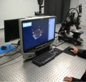
Straightforward process monitoring
Cleaner and non-contact machining
Little to no heat-affected zone, free of burr and bulging
Finer features and lines
Faster speed and precision
Consistent machining quality
No additional tooling costs by wear
No solvents or chemicals

We want to help smaller, local, custom PCB manufacturers transition from mechanical to laser. For more information or to send over samples for testing, contact one of our laser experts at sales@nsi-usa.com.


NSI Opening of Applications Laboratory

NSI Laser Announces Opening of Applications Laboratory

REMONT, California – March 29, 2017 –  NSI Laser is opening an applications laboratory at its Fremont, CA facility. This is in response to the whole electronics industry moving towards high density interconnect (HDI) and finer geometry PCBs. As new materials enter this miniaturization challenge, the demand for new and advanced laser micro machining processes increases. The new App Lab is equipped with NSI’s unique dual-head laser systems to meet these new demands. It also features analytical capabilities such as 3D imaging for real time sample process evaluation.

The App Lab will be managed by Dr. Yung Kuo, who recently joined NSI Laser as its Senior Laser Applications Engineer. Yung brings over 25 years of practical laser micro machining experience and process development. “We are delighted to launch our App Lab to better serve our prospective customers. With micro vias becoming less than 5mils, conventional PCB processes no longer apply and laser micro machining is the only option. We are ready to assist our customers in this new process development”, said Dr. Kuo.

NSI Laser is dedicated to laser micro machining and builds its systems using only state-of-the-art components. NSI systems perform a variety of processes such as etching, drilling, skiving, and routing can handle any mix and volume.

The NSI App Lab will be operational by April 3, 2017.

For additional information, please contact:
Sam Zhou
NSI Laser
48430 Milmont Dr.
Fremont, CA 94538
Phone:408-935-2270
www.nsi-usa.com
info@nsilaser.com

NSI Laser Announces Opening of Applications Laboratory