Ultra-fast lasers, more specifically femtosecond lasers, are used to assist in micromachining applications for manufacturing medical devices, glass cutting, and semiconductor, and PCB materials. Micromachining applications that once were mechanical processes and nanosecond lasers now use ultra-fast lasers. Advantages of using ultra-fast lasers for micromachining processes such as routing, skiving, drilling, and etching, are smoother walls, shapes, contours, and no heat affected zone (HAZ). HAZ is the result of heat transfer outside of the ablation zone, causing thermal damage to the material. A femtosecond laser’s process is faster than thermalization time, and will avoid inducing heat to the ablated area. This process is also known as cold micromachining.
Laser Process Examples
Cutting – Femtosecond lasers are readily used for cutting heat-sensitive and brittle material such as glass and sapphire. For example, smooth shapes can be cut out of glass and sapphire for smartphone screens, cameras, and watches. Aside from glass applications, a femtosecond laser can also cut most materials such as: ceramics, glasses, metals, polymers, and organic tissues. Because of the quality cuts, femtosecond lasers are also used for the medical industry, to cut cylindrical stents and heart valve frames.
Routing – Routing intricate patterns is more accurate with an ultra-fast laser. Creating many arches and patterns can be a challenge for flex circuit applications. Routing patterns with an ultra-fast can not only be stitched seamlessly with no burns or gaps, but saves time compared to mechanical routing and punching processes.
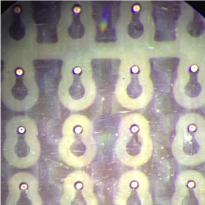
Drilling- Many industrial applications require drilling of high-quality and small geometry holes. For example, PCB manufacturers who are driving towards higher density and smaller-diameter interlayer connection holes need controlled outer and inner diameters for cylindrical holes or slightly tapered holes. An ultra-fast laser is useful in this application for shaping the holes, and result in cleaner, quality holes.
Etching – Material processing for the tough integrated circuits (IC) is significantly improved with an ultra-fast laser. Etching is a process that can be done with a wet process, dry process, or both. Using ultra-fast lasers avoids photo lithography and chemical etching to make PCB metal circuits. Dry etching has been done previously in semiconductor industry with dry etching techniques. If ultra-fast lasers can be used, that will eliminate time consuming processes, wet chemical processing, and replace all of them with a completely dry process. Anytime a wet process is replaced with a dry process, chemical and disposal costs related to wet processing are avoided. Advantages of dry etching are its reduction in human labor and material consumption.
Outlook
Using an ultra-fast laser to assist with material processes shows great potential for applications in the device integration industry. Common issues such as high surface roughness, damage to material, and inefficiency are solved with ultra-fast laser processing.
Laser assisted manufacturing processes using femtosecond lasers are still under development and new techniques are yet to emerge in today’s market. New laser processes are currently being developed and tested in NSI Laser’s applications lab. To inquire about unique laser processes for your applications or tough materials, please contact one of our laser specialists at info@nsilaser.com