Hybrid Material Processing

In this week’s blog, we’re going to discuss our experience processing hybrid material. When you’re trying to determine which laser to run preliminary sample testing, you must first consider these variables first:

Is your hybrid material uniformly or randomly distributed?

Randomly distributed composite will be more challenging and time consuming when developing a recipe.

Is the material composite similar or very different from each other?

When a material is significantly different from each other, there might be a need to develop very different processes to deal with each composite material. Sometime this requires 2 different laser types to accomplish all the objectives. NSI specifically designed the Dual Beam line to cater to this requirement.

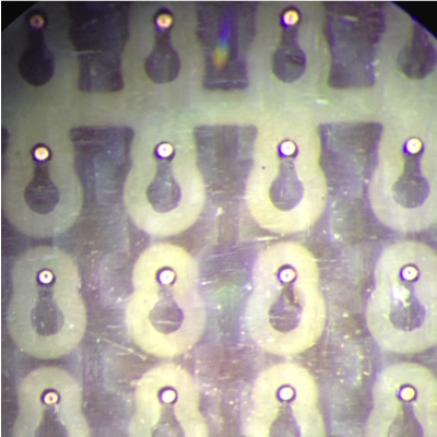
What are the key objectives (Small HAZ, Smooth Walls, Controlled OD/ID, etc.) you’re trying to achieve in this laser process?

Knowing you must have and nice to have process output requirements is key in determining which laser system is best suited for you. Let’s take a comparison between Femtosecond and Nanosecond lasers.

1. Throughput for fs lasers can be 3x less than ns lasers. To offset this throughput issues, we have utilized our dual beam laser systems. For large volume removal (holes >50 um diameter and >50 um depth) a ns laser could be used first to remove a large portion of the material and then a fs laser can be used for “clean-up” run.

2. For Ultrafast (ps or fs) lasers, assuming the total energy is the same, will have much higher peak power and energy density than the ns laser has. This will result with almost all the energy of the ultrashort pulse contributing to the material interaction and no heat generation or transferring onto the material.

3. Ultrafast lasers are significantly more expensive than ns lasers, usually 3x or greater.

Is your process critical enough to require an absorption test on the material?

When you’re having an issue accomplishing a specific output, you can consider sending the material to a lab to perform absorption testing to determine which wavelength and pulse width is best suited for each of your hybrid material.

Hybrid Material Processing

Posted in: Blog

Transitioning From Mechanical to Laser Micro Machining

Laser processing systems are costly due to the expensive components and the laser itself. Don’t be scared by the price tag though, there are ways to go around it such as special financing or purchasing older generation or refurbished systems. If there aren’t any available used or refurbished options, opt towards dual laser for more versatility. One system with a combination of lasers enable multiple processes in one set-up and will save costs compared to buying two lasers and will enhance your material processing capability if you use two different wavelengths and laser types.

Return On Investment
It might be a good investment to buy an inhouse laser system if there’s such a high demand that almost all the jobs have to be sent out. Eventually, the cost of the outsourcing all the jobs will exceed the price of an actual system. Getting an in-house system will shorten lead time, save money, and increase competitive advantage. It is more beneficial for the growth of the company to have the micro machining capabilities in house.

Advantages of laser processing:

Controllable depth and inner/outer diameter
Straightforward process monitoring
Cleaner and non-contact machining
Little to no heat-affected zone, free of burr and bulging
Finer features and lines
Faster speed and precision
Consistent machining quality
No additional tooling costs by wear
No solvents or chemicals

We want to help smaller, local, custom PCB manufacturers transition from mechanical to laser. For more information or to send over samples for testing, contact one of our laser experts at sales@nsi-usa.com.


Laser Processing: Ultra-fast lasers

Ultra-fast lasers, more specifically femtosecond lasers, are used to assist in micromachining applications for manufacturing medical devices, glass cutting, and semiconductor, and PCB materials. Micromachining applications that once were mechanical processes and nanosecond lasers now use ultra-fast lasers. Advantages of using ultra-fast lasers for micromachining processes such as routing, skiving, drilling, and etching, are smoother walls, shapes, contours, and no heat affected zone (HAZ). HAZ is the result of heat transfer outside of the ablation zone, causing thermal damage to the material. A femtosecond laser’s process is faster than thermalization time, and will avoid inducing heat to the ablated area. This process is also known as cold micromachining.

Laser Process Examples

Cutting – Femtosecond lasers are readily used for cutting heat-sensitive and brittle material such as glass and sapphire. For example, smooth shapes can be cut out of glass and sapphire for smartphone screens, cameras, and watches. Aside from glass applications, a femtosecond laser can also cut most materials such as: ceramics, glasses, metals, polymers, and organic tissues. Because of the quality cuts, femtosecond lasers are also used for the medical industry, to cut cylindrical stents and heart valve frames.

Routing – Routing intricate patterns is more accurate with an ultra-fast laser. Creating many arches and patterns can be a challenge for flex circuit applications. Routing patterns with an ultra-fast can not only be stitched seamlessly with no burns or gaps, but saves time compared to mechanical routing and punching processes.

Drilling- Many industrial applications require drilling of high-quality and small geometry holes. For example, PCB manufacturers who are driving towards higher density and smaller-diameter interlayer connection holes need controlled outer and inner diameters for cylindrical holes or slightly tapered holes. An ultra-fast laser is useful in this application for shaping the holes, and result in cleaner, quality holes.

Etching – Material processing for the tough integrated circuits (IC) is significantly improved with an ultra-fast laser. Etching is a process that can be done with a wet process, dry process, or both. Using ultra-fast lasers avoids photo lithography and chemical etching to make PCB metal circuits. Dry etching has been done previously in semiconductor industry with dry etching techniques. If ultra-fast lasers can be used, that will eliminate time consuming processes, wet chemical processing, and replace all of them with a completely dry process. Anytime a wet process is replaced with a dry process, chemical and disposal costs related to wet processing are avoided. Advantages of dry etching are its reduction in human labor and material consumption.

Outlook

Using an ultra-fast laser to assist with material processes shows great potential for applications in the device integration industry. Common issues such as high surface roughness, damage to material, and inefficiency are solved with ultra-fast laser processing.

Laser assisted manufacturing processes using femtosecond lasers are still under development and new techniques are yet to emerge in today’s market. New laser processes are currently being developed and tested in NSI Laser’s applications lab. To inquire about unique laser processes for your applications or tough materials, please contact one of our laser specialists at info@nsilaser.com

Introduction to laser micro-machining

Introduction to Laser Micro-Machining – PCB Drilling

Overview:

Laser micro machining includes laser ablation, surface structuring of tough materials, and routing to create wave-guides. Materials suited for laser ablation include: ceramics, glasses, metals, polymers, and semiconductors. Typical laser micro machining is done with pulses with a duration of nanoseconds to picoseconds. Nanosecond laser processing. Ultra-fast lasers have pulses shorter than picoseconds, even as short as femtoseconds.

laser micro machining

Fig 1. Dual-head UV/CO2 laser micro-machine for PCB drilling, skiving and routing

To achieve high quality results from laser micro machining, an optimum laser process must be chosen. This starts with the choice of the laser itself. The process optimization comes from many parameters, including laser wavelengths, power, pulse fluence and duration, and beam size. Additional considerations include work area to be covered, acceptable process time and handling the debris that is generated by the ablation.

Each material to be laser micro machined has its own unique response. Therefore, the processsteps must be tailored for each material to be processed. For example, one material might be much more impervious to heat than another. This will impact both power and pulse duration. For materials that are extremely sensitive to heat buildup, an ultra-fast laser may be the only option.

PCB drilling:

Today’s multilayer PCBs feature both through holes and via holes. Through holes typically have diameters of 5mils or larger and they are the deepest holes; hence they have high aspect ratios and are most conveniently mechanically drilled. Via holes are either blind vias or buried vias. Blind vias are exposed to one side of the board and stop at the next underlying copper layer. Buried vias start out as blind vias, and are thereafter embedded in the multilayer PCB connecting the two copper layers intermittent in the multilayer PCB structure. This is accomplished by stacking multilayers together. The challenge for any via is to drill through the first copper layer, then drill through the underlying composite material, for example (FR4) without damaging the next copper layer. NSI Laser has developed a dual-head UV/CO2 system to address this exact challenge. The UV laser drills though the first copper layer, but only marginally into the FR4. The CO2 laser is the most suitable for the FR4, and many other composite materials typically used in PCBs. The most unique feature with the CO2 laser light is that it stops at the second copper layer. The two lasers can operate simultaneously on different parts of the panel PCB panel reducing the overall drilling process time.

Fig. 2 Blind via (1 mil – 25um) at 500x magnification

Creating via holes by conventional mechanical drilling technology can only be done by careful control of the height. The less the hole diameter, the more difficult mechanical drilling becomes. Another challenge is the aspect ratio (hole diameter to hole depth). Mechanical drilling is highly suitable for for deep holes with aspect ratios much larger than 1:1. However, when the hole diameter goes below 4mils (100microns), mechanical drilling becomes physically impossible.

By comparison, with laser drilling the smaller the hole diameter, the deeper the hole. This is increasingly valuable as today’s high density PCBs require smaller and smaller via holes. Thus, laser drilling has gaining in popularity. And this trend is growing as even higher density PCBs become necessary to accommodate even more electronic circuitry over a small area. Laser drilling offers a long pathway of opportunities with many more parameters which can impact the drilling. Not until hole diameters and PCB layer thicknesses approach the micron level will today’s laser drilling reach its physical limits.