NSI Laser Announces Opening of Applications Laboratory
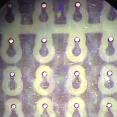
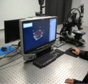
REMONT, California – March 29, 2017 – NSI Laser is opening an applications laboratory at its Fremont, CA facility. This is in response to the whole electronics industry moving towards high density interconnect (HDI) and finer geometry PCBs. As new materials enter this miniaturization challenge, the demand for new and advanced laser micro machining processes increases. The new App Lab is equipped with NSI’s unique dual-head laser systems to meet these new demands. It also features analytical capabilities such as 3D imaging for real time sample process evaluation.
The App Lab will be managed by Dr. Yung Kuo, who recently joined NSI Laser as its Senior Laser Applications Engineer. Yung brings over 25 years of practical laser micro machining experience and process development. “We are delighted to launch our App Lab to better serve our prospective customers. With micro vias becoming less than 5mils, conventional PCB processes no longer apply and laser micro machining is the only option. We are ready to assist our customers in this new process development”, said Dr. Kuo.
NSI Laser is dedicated to laser micro machining and builds its systems using only state-of-the-art components. NSI systems perform a variety of processes such as etching, drilling, skiving, and routing can handle any mix and volume.
The NSI App Lab will be operational by April 3, 2017.
For additional information, please contact:
Sam Zhou
NSI Laser
48430 Milmont Dr.
Fremont, CA 94538
Phone:408-935-2270
www.nsi-usa.com
info@nsilaser.com