Introduction to Laser Micro-Machining – PCB Drilling
Overview:
Laser micro machining includes laser ablation, surface structuring of tough materials, and routing to create wave-guides. Materials suited for laser ablation include: ceramics, glasses, metals, polymers, and semiconductors. Typical laser micro machining is done with pulses with a duration of nanoseconds to picoseconds. Nanosecond laser processing. Ultra-fast lasers have pulses shorter than picoseconds, even as short as femtoseconds.

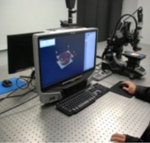
Fig 1. Dual-head UV/CO2 laser micro-machine for PCB drilling, skiving and routing
To achieve high quality results from laser micro machining, an optimum laser process must be chosen. This starts with the choice of the laser itself. The process optimization comes from many parameters, including laser wavelengths, power, pulse fluence and duration, and beam size. Additional considerations include work area to be covered, acceptable process time and handling the debris that is generated by the ablation.
Each material to be laser micro machined has its own unique response. Therefore, the processsteps must be tailored for each material to be processed. For example, one material might be much more impervious to heat than another. This will impact both power and pulse duration. For materials that are extremely sensitive to heat buildup, an ultra-fast laser may be the only option.
PCB drilling:
Today’s multilayer PCBs feature both through holes and via holes. Through holes typically have diameters of 5mils or larger and they are the deepest holes; hence they have high aspect ratios and are most conveniently mechanically drilled. Via holes are either blind vias or buried vias. Blind vias are exposed to one side of the board and stop at the next underlying copper layer. Buried vias start out as blind vias, and are thereafter embedded in the multilayer PCB connecting the two copper layers intermittent in the multilayer PCB structure. This is accomplished by stacking multilayers together. The challenge for any via is to drill through the first copper layer, then drill through the underlying composite material, for example (FR4) without damaging the next copper layer. NSI Laser has developed a dual-head UV/CO2 system to address this exact challenge. The UV laser drills though the first copper layer, but only marginally into the FR4. The CO2 laser is the most suitable for the FR4, and many other composite materials typically used in PCBs. The most unique feature with the CO2 laser light is that it stops at the second copper layer. The two lasers can operate simultaneously on different parts of the panel PCB panel reducing the overall drilling process time.

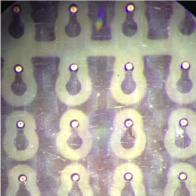
Fig. 2 Blind via (1 mil – 25um) at 500x magnification
Creating via holes by conventional mechanical drilling technology can only be done by careful control of the height. The less the hole diameter, the more difficult mechanical drilling becomes. Another challenge is the aspect ratio (hole diameter to hole depth). Mechanical drilling is highly suitable for for deep holes with aspect ratios much larger than 1:1. However, when the hole diameter goes below 4mils (100microns), mechanical drilling becomes physically impossible.
By comparison, with laser drilling the smaller the hole diameter, the deeper the hole. This is increasingly valuable as today’s high density PCBs require smaller and smaller via holes. Thus, laser drilling has gaining in popularity. And this trend is growing as even higher density PCBs become necessary to accommodate even more electronic circuitry over a small area. Laser drilling offers a long pathway of opportunities with many more parameters which can impact the drilling. Not until hole diameters and PCB layer thicknesses approach the micron level will today’s laser drilling reach its physical limits.